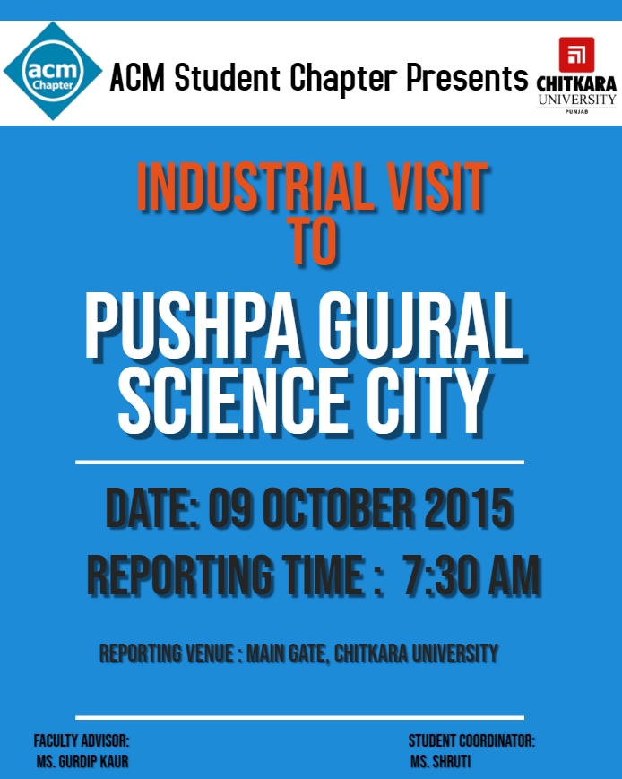
INDUSTRIAL VISIT

ACM Student Chapter organized industrial visit to Semi Conductor Laboratory, Mohali on 30th September 2015. Only 2 of our students (Rajat Sharma and Shubham Singla) got a chance to visit the site. In the first section, they went to Class 1 Zone, where they were shown how the fabrication of a wafor takes place which gave them the idea about the initial step for an IC production and how the base layer deposition, electrical layer deposition and sacrificial removal process takes place. In the second section students were taken to the R&D Department. Here they came to know about various techniques to design an IC through VHDL. Next they were taken to de-ionised water plant where they were the process to de-ionise the water and to bring down the resistivity of the water. Lastly they were taken to class 100 they were shown the packaging process of an IC by soldering or by manual installment of a wafor the package.
The head of department also told them how they planned to upgrade the fab after IBM backed out the deal and how SCL was undergoing an upgrade to produce chips of 0.18 micrometers from tower semiconductor, Israel. The students interacted with the officials and gained a lot of knowledge which will be useful for them in their academic.


